










TSMC and Samsung Foundry are the only two foundries currently offering 3nm and 4nm class process technology to customers. However, the business media occasionally accuse Samsung Foundry of mediocre yields of unverified cutting-edge nodes. However, according to a recent report issued by an investment banking firm, Samsung’s 3nm and 4nm class node yields are at fairly decent levels. But there are pitfalls.
Samsung Foundry’s 4 nm class process technology yield is now over 75%. In contrast, the yield of SF3E (3nm class, early gate all-around) chips is currently over 60%, according to a report by Hi Investment & Securities, a member of DGB Financial Group, he said at Kmib.co.kr. reports. . The same report claims yields at TSMC’s N4 node are approaching 80%, but again this is an estimate by the researchers.
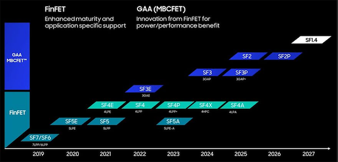
Foundry yield information is generally not verifiable. Because yield depends on several factors such as die size, performance targets, and design peculiarities, chip contract manufacturers never publicly talk about yield. Sometimes they publish defect densities compared to previous nodes, but that’s hardly true for Samsung Foundry’s his SF4E, SF4, SF4P, and his SF3E.
Samsung Foundry has only officially stated that its SF3E process technology is being mass-produced with stable yields (presumably to address media reports late last year that SF’s SF3E yields were erratic). Development of purified SF3 is ongoing. .
”We have mass-produced the 1st generation 3nm process with a stable yield, and based on this experience, we are proceeding with the development of the 2nd generation process to secure further mass production capability.,” Samsung said in a statement.
On the other hand, TechInsights found One of the first chips made on Samsung’s SF3E process. It appears to be a Whatsminer M56S++, a cryptocurrency mining chip from Chinese developer MicroBT. A mining chip is a small, simplified device with a regular structure and a small number of SRAM bit cells. Chips like this are easy to manufacture and work perfectly as pipe cleaners for modern process technology, so it’s no surprise that Samsung Foundry makes chips instead of bulky ASICs on SF3E. On the other hand, the yield of small chips is naturally higher than that of large ASICs manufactured on the same node. So even if Whatsminer M56S++ has a yield of 75% or more, it doesn’t mean that the yield of his SoC in bigger smartphones or his PC will be at the same level with the same defect density.
It was indirectly confirmed that the yield of Samsung’s 5nm and 7nm class manufacturing process is improving. A DigiTimes article cited Samsung foundry utilization for its 5nm line rising to 80%, with combined 5nm and 7nm fab utilization recently rising to 90%, and 60% by 2022. said to have risen from ET News. Again, information is from unofficial sources.
Usually, fabless chip designers don’t tend to use nodes with high defect density, so if the 5 nm class (Samsung’s SF4, which is derived from SF5) sees higher usage, this is likely to make them more likely to be used by Samsung customers. It may indicate intensive use. Alternatively, this could indicate that the Samsung Foundry has customers desperate to increase production despite low yields due to high demand. However, given the current market conditions, that may not be the case.
Source: Kmib.co.kr, DigiTimes, TechInsights